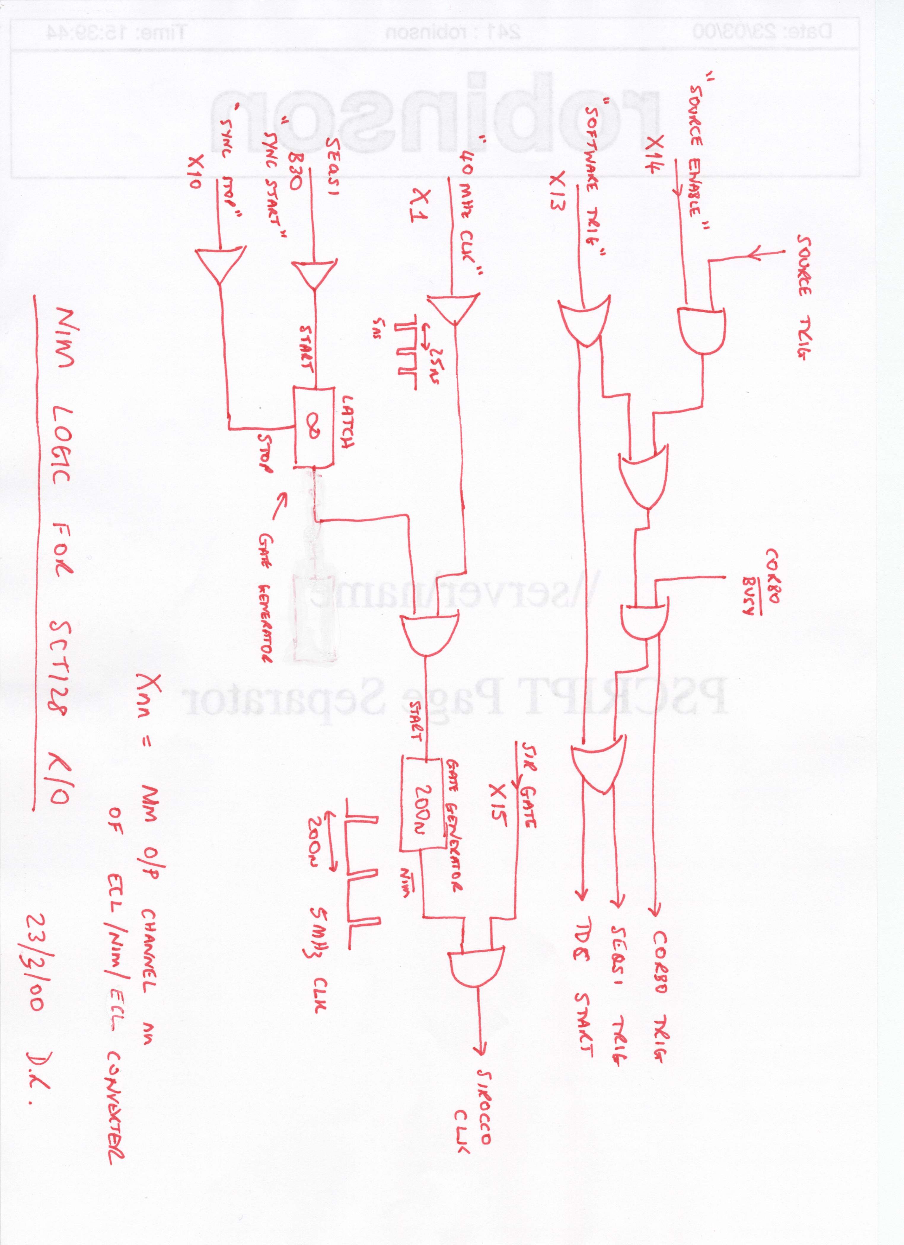
A very (very) rough hand-drawn logic diagram should be visible here:
You must set up the following cabling. You can change the software to
modify the cabling at your own risk.
SEQSI
Pin Nos
ECL/NIM/ECL Pin Number
of J1
Description
Chan
SEQSI PL2 LRS4616 Chan No
Connector on sct board (output(s) used from ecl/nim/ecl)
(starts from 0) (starts from 1) (starts from
1) (starts
from 1)
clock
46,47
1
1,2
Clock - ecl to chip, nim to logic
4
9,10
3
5,6
Reset - ecl to chip
5
11,12
4
7,8
Polarity - ecl to chip
6
13,14
5
9,10
Address - ecl to chip
7
15,16
6
11,12
tstenable - ecl to chip, not used?
8
17,18
7
13,14
command - ecl to chip
9
19,20
8
15,16
singread 0- ecl to chip
10
21,22
9
17,18
muxtstenable - ecl to chip, not used?
11
23,24
10
n/a
sirocco strobe (sync stop) - nim to logic
12
25,26
11
n/a
not used
13
27,28
12
n/a
trsynchro - not used (historical)
14
29,30
13
n/a
sofware trigger - nim to logic
15
31,32
14
n/a
enable source trigs - nim to logic
16
33,34
15
n/a
sirocco gate - nim to logic
17
35,36
16
n/a
TDC stop - ECL to TDC module
30 (nim o/p) n/a
n/a
n/a
sirocco strobe (sync start) to nim logic
NIM logic
A very (very) rough hand-drawn logic diagram should be visible here: